
Why GaN for DC-DC Space Designs

- Home
- /
- POSTS
- /
- Technology
- /
- Why GaN for DC-DC...
![]() Power electronics engineers are constantly working towards designs with higher efficiency and higher power density while maintaining high reliability and minimizing cost. Advances in design techniques and improved component technologies enable engineers to consistently achieve these goals.
Power electronics engineers are constantly working towards designs with higher efficiency and higher power density while maintaining high reliability and minimizing cost. Advances in design techniques and improved component technologies enable engineers to consistently achieve these goals.
Power semiconductors are at the heart of these designs and their improvements are vital to better performance.
In this EPC space blog, we will demonstrate how GaN power semiconductors allow for innovation in the harsh radiation environments of space applications.
GaN power semiconductors offer designers in the high reliability market a sudden and significant improvement in electrical performance over their silicon power MOSFET predecessors.
Table 1 compares radiation hardened GaN and Si power semiconductor device characteristics important for circuit designers to increase efficiency and power density in their converter.
| 200 V GaN FBG20N18B | 200 V Si MOSFET | Technology Comparison | |
| VDS (V) | 200 | 200 | Same |
| RDS(ON) (mΩ) | 26 | 28 | Similar |
| Device Area (mm2) | 23 | 237 | 10 x Reduction |
| QG (nC) | 6 | 240 | 40 x Reduction |
| QGD (nC) | 2 | 60 | 30 x Reduction |
| QGS (nC) | 2 | 70 | 35 x Reduction |
| COSS (pF) @50 V VDS | 300 | 900 | 3 x Reduction |
| COSS (pF) @1 V VDS | 950 | 10000 | 10 x Reduction |
| QRR (nC) | 0 | 11700 | Infinite Reduction |
| VSD (V) | 1.75 | 1.2 | 1.5 x Increase |
While the comparisons in Table 1 clearly show the benefits of a new power semiconductor technology, it is hard to estimate how this will translate into real world circuit performance where the power semiconductor is part of a larger system. We will explain the theoretical impact of these device characteristics on converter performance using the power semiconductor commutation diagram in Figure 1 and describe the impacts on an innovative real-world product design using the VPT SGRB10028S DC-DC converter, shown in Figure 2.
The SGRB10028S has a 100 V input, an adjustable single output from 12 V to 28 V, output power up to 400 W, and efficiencies above 96%. The SGRB Converter employs a Phase-Shifted Full Bridge circuit topology with GaN devices used for both the primary devices and the secondary synchronous rectifiers.
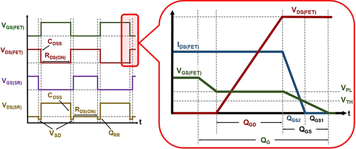
Starting from the first entry in Table 1, VDS, the maximum drain-to-source blocking voltage of the power semiconductor. VDS must be large enough to support the off-state drain-to-source voltage shown in Figure 1 with adequate margin; this also includes circuit voltage ringing, introduced mainly by parasitic inductances in the circuit.
Most of the blocking voltage is dependent on the isolation transformer leakage inductance spike and the design input and output voltages. Thus, for GaN and Si designs, the voltage stresses, and therefore maximum drain-to-source blocking voltage will be the same.
Combining advanced GaN power semiconductors and state of the art design techniques enables a new level of performance in high reliability space designs as demonstrated in Figure 2.
The VPT SGRB series have been designed specifically for space-borne telecommunications where high efficiency, low noise, and radiation tolerance are imperative. Using advanced GaN-based technology, the SGRB series was developed to provide a solution that increases power supply efficiency, resulting in reduced system size, weight, and cost.
This GaN-based SGRB series of DC-DC converters earned the Military & Aerospace Electronics Innovators Awards Platinum recognition, its highest honor. This distinction recognizes companies in the aerospace and defense electronics industries that have made groundbreaking contributions and innovative solutions to solve design challenges.


