+39 334 9529 414
info@microrel.com

UMS Foundry training methodologies for GaN and GaAs technologies
UMS Foundry training methodologies for GaN and GaAs technologies

  1. Home
  2. /
  3. POSTS
  4. /
  5. RF Microwave
  6. /
  7. UMS Foundry training methodologies...

United Monolithic Semiconductors (UMS) organises regular training for clear understanding of Technology Processes, Design flow and Techniques to realise effective designs using UMS latest toolkits.

Course Objectives

The objective of this Foundry training is to equip attendees with the optimal methodologies for utilising UMS GaN and GaAs technologies for RF and mmWave MMIC applications.

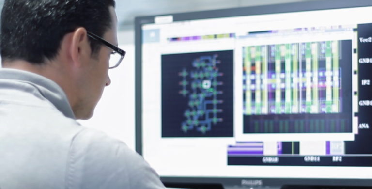
This session will equip RF designers with the knowledge and skills to utilise the UMS PDKs effectively in circuit design.

The session will also address GaAs and GaN wafer fabrication in order to provide attendees with a deeper familiarity with III-V technologies. The important modelling topics are also addressed from both an electrical and thermal perspective. The content of our PDKs is also discussed, and demonstrations are provided with the support of Keysight and Cadence engineers.

Experienced UMS designers will deliver lectures on the following topics: LNA design, HPA design and mixer design(*). Examples are provided and discussed in detail.


The foundry flow, layout rules and specifications related to GaN are also addressed. A lecture is given on process qualification and the space level. All available back-end activities (on wafer test, dicing and picking) are discussed prior to a BE tour.

The training is completed with a discussion on different packaging solutions developed at UMS.

Course content

The 3-day standard Foundry course is  held at regular intervals in our Villebon/Yvette facility.

Typically, the course covers the following topics:

  • GaAs and GaN Technologies
  • Thermal and electrical modelling
  • Layout skills and CAD demo with Keysight and Cadence
  • Specific techniques for Mixer, High Power Amplifier and Low Noise Amplifier design
  • On-wafer measurement and Back-End description
  • Reliability and Space qualification
  • How to get the best out of our foundry service
  • Packakging: discussion of possibilities around a presentation of hardware solutions
  • Open forum and specific questions

Joining a course

If you wish to attend  or need further information on foundry courses, please contact mktsales@ums-rf.com

Our team remains at your disposal for any further questions.


Contacts:

United Monolithic Semiconductors
Bât. Charmille – Parc Mosaic – 10, Avenue du Québec – 91140 VILLEBON-SUR-YVETTE – France
Tel.: +33 (0) 1 69 86 32 00 – www.ums-rf.com

ITALY Agent : DANILO LAUTA
MICROREL – Via Guido Rossa 34, CP.00065 – Fiano Romano, ROME, ITALY
Email: danilo.lauta@microrel.com
Phone : +39 334 9529414
Web: www.microrel.com